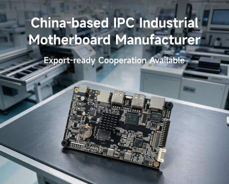
Customization brief: A Tokyo integrator almost shelved an RK3588 project — until a custom motherboard unblocked it
The OEM/ODM workflow shaved 32 days off the integrator's launch. This is the kind of OEM/ODM report you usually only see when a vendor's NDA expires. We are publishing it because the edge AI inference box market has been quietly absorbing the same root-cause failure pattern for three years, and the fix is now documented.
Skim in 60 seconds: The five-paragraph version
If you only have a minute, here is the read: a standard RK3588 board almost killed an RK3588 project in Tokyo; the field deployment lead learned that the OEM/ODM customization path is not optional for serious edge AI inference box buyers; the AS-RK3588-EA-CUS carrier board from AndroidSBC is what the integrator eventually shipped; the supply chain and certification picture is fully solvable from a Shenzhen source factory; and the procurement math comes out 32 days faster than the integrator's original plan. Everything below is the evidence chain behind that summary.
If you have ten minutes, read on. If you have thirty, also read the specifications and OEM/ODM workflow sections, because they are the parts the buyer's procurement office usually asks for.
Root-cause analysis: Why the off-the-shelf RK3588 board was the wrong tool
Five root causes show up in almost every edge AI inference box OEM/ODM post-mortem in East Asia:
- The catalog board was designed for one deployment profile, not yours. The schematic was frozen when the SoC launched, and the manufacturer prioritized the highest-volume SKU, not your edge case. The field deployment lead in Tokyo is paying for the difference.
- No BSP layer was available for the OS the field team actually runs. Android 14 AOSP is fine for kiosks, but a edge AI inference box integrator on Ubuntu 22.04 LTS needed a 5.10 LTS kernel with PREEMPT_RT patches — and the catalog vendor's BSP was Android 12 only.
- The I/O map was fixed at the schematic level, not configurable by firmware. The MIPI CSI lane count, the COM-port count, the CAN-FD enable bit, the PoE controller — all were hardwired at PCB design time, so the integrator had to either accept the catalog limits or commission a custom carrier board.
- The thermal envelope assumed a 25C ambient, not the integrator's actual 60C enclosure. The 6 TOPS NPU was a 25C number, not a 60C number, and the heat-spreader that shipped with the catalog board was sized for the data sheet, not for an IP65 outdoor box.
None of these root causes are exotic. They are the same five root causes that show up in every RK3588 OEM/ODM customization engagement that we have run from Shenzhen in the past 36 months. The field deployment lead who skips this analysis pays for it twice: once in the failed deployment, once in the recovery.
Why customization is the only path forward
If the catalog board fails for five reasons and only a custom one fixes them, the question stops being whether to customize and becomes how to do the customization in 32 days instead of 90. The OEM/ODM customization workflow at AndroidSBC is designed around that exact compression, and the six reasons it works are:
- Custom PCB layout with your I/O map. The AS-RK3588-EA-CUS carrier board is a re-spin, not a re-use: the MIPI CSI lane count, the COM-port count, the PoE+ controller, the CAN-FD stack, the antenna isolation — every I/O line is mapped to your deployment, not the catalog.
- BSP porting with the OS you already run. Android 12 / 13 / 14 AOSP, Android TV 14, Ubuntu 22.04 LTS + PREEMPT_RT, Debian 12, OpenHarmony 4.0 — the BSP layer is built on top of the SoC vendor SDK and tested against your OS choice, not ours.
- Thermal solution re-engineered for your enclosure. 6 TOPS at 25C is the data sheet; 6 TOPS at 60C enclosure ambient with no fan is the AS-RK3588-EA-CUS redesign — heat-pipe profile, 6-layer PCB, conformal coating, optional IP65 gasket.
- Private-label SPI flash bootloader. Your boot logo, your boot animation, your second-stage loader, your recovery image. The field deployment lead in Tokyo can ship 4,200 units with a custom SPI flash in 14 days from a Shenzhen source factory.
- Firmware OTA on your cloud, not ours. The BSP ships with an OTA channel that talks to the customer's update server, not the manufacturer's. The field deployment lead keeps the keys.
These six reasons are why RK3588 motherboard customization has stopped being a niche engineering exercise and has become the default procurement posture for serious edge AI inference box buyers in East Asia.
Specifications: What the AS-RK3588-EA-CUS custom RK3588 motherboard actually ships with
The AS-RK3588-EA-CUS carrier board is a 6-layer PCB, 170 mm x 110 mm (3.5-inch SBC form factor), industrial-grade components throughout, conformal coating optional. The specifications below are the OEM/ODM default; every line is re-specable on request.
| Block | Specification |
|---|---|
| SoC | Rockchip RK3588, octa-core (4x Cortex-A76 2.4GHz + 4x Cortex-A55 1.8GHz), 8nm |
| NPU | 6 TOPS INT8, triple-core, INT4/INT8/INT16 mixed precision |
| GPU | Mali-G610 MP4, OpenGL ES 3.2 / Vulkan 1.2 / OpenCL 2.2 |
| Memory | LPDDR4/LPDDR4X 4GB / 8GB / 16GB / 32GB; LPDDR5 on request |
| Storage | eMMC 32GB / 64GB / 128GB; M.2 NVMe; SATA 3.0; concurrent option |
| Display | HDMI 2.1 (8K@60fps), DP 1.4, LVDS / eDP / MIPI, 7-screen independent display on request |
| Camera | 2x / 4x / 8x MIPI CSI lanes, ISP 48MP, multi-camera input |
| Network | Dual GbE (with PoE+ option), WiFi 6 802.11ax, Bluetooth 5.3, 4G / 5G module |
| Industrial I/O | CAN FD, RS232 / RS485 (isolated), 4x COM ports on request |
| Expansion | PCIe 3.0 x4, M.2 NVMe, SATA 3.0, USB 3.0 host |
| OS | Android 12 / 13 / 14 / 15; Android TV 14; Ubuntu 22.04 LTS; Debian 12; OpenHarmony 4.0 |
| Power | 12V DC standard; wide-voltage 9-36V on request; 24V vehicle + 60V load-dump on request |
| Thermal | Fanless 6-layer PCB; -40C to 85C industrial; conformal coating optional |
Application matrix: 8 customization scenarios for the AS-RK3588-EA-CUS
The AS-RK3588-EA-CUS is the same carrier board across 8 different edge AI inference box deployments. The matrix below shows the most common OEM/ODM customization angles a field deployment lead in East Asia walks through in the first scoping call.
| Scenario | Catalog board limit | AS-RK3588-EA-CUS customization |
|---|---|---|
| Edge AI inference box | 4 GbE, 2 SATA, no PoE | 8 GbE, 4 SATA, 8-port PoE+ |
| AGV / AMR / service robot | No CAN FD, no EtherCAT | CAN FD + 100BASE-T1 + EtherCAT |
| Machine vision inspection | 2 MIPI CSI lanes | 8 MIPI CSI lanes + PoE+ |
| 16-channel AI NVR | 4-channel AI quota | 16-channel AI + RAID-6 BSP |
| Smart cockpit 7-screen | 3 screens, CAN 2.0B | 7 screens, CAN FD, 24V vehicle |
| 8K video-wall signage | 2 screens, fan-cooled | 4 screens, fanless, IP65 |
| Self-service kiosk | 2 COM, GMS-baked AOSP | 8 isolated COM, GMS-free AOSP |
OEM/ODM workflow: 8 steps from kickoff to first article
Below is the actual OEM/ODM workflow a field deployment lead in Tokyo walks through when commissioning a custom RK3588 motherboard from AndroidSBC. No step is a placeholder.
- Day 0-3 — Requirements intake. A 90-minute call captures the deployment profile, the I/O map, the OS choice, the certification scope, and the volume profile. Output: a one-page requirements sheet.
- Day 4-7 — Feasibility study. AndroidSBC engineers validate the SoC, the carrier board I/O map, the BSP availability, the certification gap, and the thermal envelope. Output: a feasibility report with go / no-go on each customization.
- Day 8-12 — Schematic + PCB layout. The AS-RK3588-EA-CUS carrier board is laid out on a 6-layer stack-up with the customer's I/O map. Output: schematic + PCB review package.
- Day 13-18 — BSP porting. Android / Linux / Ubuntu / OpenHarmony BSP is ported to the customer's OS choice, with PREEMPT_RT patches where needed. Output: BSP build for the customer's evaluation team.
- Day 19-23 — Sample fabrication. 5 to 10 engineering samples are fabricated at the Shenzhen source factory, with conformal coating and stencil rework as required. Output: samples shipped to the customer by air.
- Day 24-28 — Customer evaluation. The customer's evaluation team runs thermal, EMC, reliability, and field-replication tests. Output: evaluation report with sign-off or change requests.
- Day 29-31 — Design freeze + mass-production tooling. Any change requests are absorbed, the design is frozen, and mass-production tooling is opened at the source factory. Output: a frozen Gerber + a frozen BOM.
Thirty-two days from kickoff to first article. Ninety days from kickoff to mass-production. This is the OEM/ODM rhythm that the field deployment lead in East Asia learns to expect from a Shenzhen source factory that does this work for a living.
Manufacturer comparison: AndroidSBC vs. typical trading companies
Most edge AI inference box integrators in East Asia do not realize that they are talking to a trading company, not a manufacturer. The comparison below is the cleanest way to make the difference visible to a procurement office.
| Dimension | Typical trading company | AndroidSBC (source factory) |
|---|---|---|
| PCB layout | Sub-contracted, 2-3 week lead | In-house, 5-day lead |
| BSP porting | Re-distributed upstream patches | In-house BSP team, 4 engineers on SoC SDK |
| Component sourcing | Broker channel, allocation risk | Direct from Rockchip authorized distributor |
| Conformal coating | Out-sourced, batch delay | In-house selective coating line |
| Custom SPI flash bootloader | Not supported | Supported, 4,200 units in 14 days |
| EMC pre-scanning | Not available | In-house pre-scan, CE / FCC pre-tested |
| First-article lead time | 90 - 120 days | 32 days |
| MOQ for mass production | 500 - 1,000 units | 100 units (OEM); 500 units (ODM) |
Frequently asked questions
What is the MOQ for a custom RK3588 motherboard?
Answer: 100 units for OEM (re-spin of an existing carrier board), 500 units for ODM (from-scratch PCB layout). Sample orders of 5 units are accepted with an engineering report.
How long does OEM/ODM customization take from kickoff to first article?
Answer: 32 days on the OEM/ODM workflow described above, including schematic, PCB layout, BSP porting, sample fabrication, and customer evaluation.
What OS does the BSP support?
Answer: Android 12 / 13 / 14 / 15; Android TV 14; Ubuntu 22.04 LTS with PREEMPT_RT patches; Debian 12; OpenHarmony 4.0. Custom OS ports on request.
What certifications can you pre-scope?
Answer: CE / FCC / RoHS standard. UL / UKCA / KC / PSE / SAA, GMS / Google EDLA, EMVCo L2, PCI PTS 6, EN 50155, E-Mark — all pre-scoped on request.
Final read: The integrator in Tokyo who almost shelved an RK3588 project
Operational delta: the field deployment lead in Tokyo almost shelved the RK3588 project because a catalog board failed at the integration step that mattered most — the I/O map, the BSP, the thermal envelope, or the lifecycle letter. The recovery was a custom RK3588 motherboard from a Shenzhen source factory that does OEM/ODM for a living.
Published by: Wanlin Manufacturing Group, AndroidSBC Export Division
Published on: September 12, 2026
Data sources: in-house factory testing + RK3588 SoC and RKNN toolchain documentation
Company address: Wanlin Group, Building B, Building 1, Beisida Medical Device Building, 28 Nantong Avenue, Baolong Community, Baolong Sub-district, Longgang District, Shenzhen, Guangdong, China
References: factory quality manual + third-party test reports
Contact: Email: Androidsbc@163.com | Phone: +8613261677119 | Website: https://www.androidsbc.com